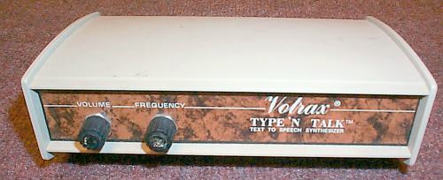
Okay. So for this Type 'n Talk thing to work, I need to design a schematic. Then I can lay out a board, then get it made, populate it, etc..
Decided to give
Fritzing a go. It's an interesting, relatively new electronics design software that's open-source and seems fairly friendly. I don't think it has an autorouter, but that's no problem, I can lay out the traces myself; there's not too many of them on this board. I'm combining components too, so that should reduce part count and traces even further.
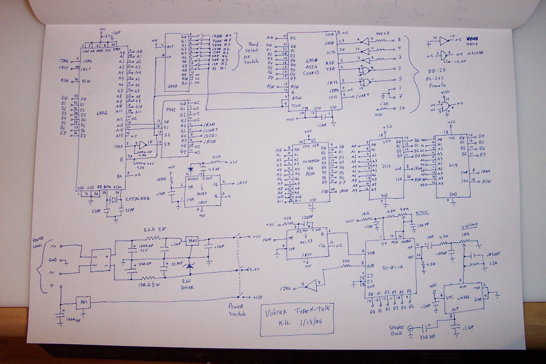
So, to give you an idea of what I need to do, I need to take
this schematic, and create my own with new parts that I can actually get, and make it actually work.
The first thing I decided to tackle is the ICs. I don't know what a lot of these ICs are, I've never used them before. A lot of electronics veterans may know about them from seeing or using them in the past, but I'm new to this game. What's a 2114? a 6802? a 7442? Well, they used to be some industry standard parts. Every manufacturer made their own version of them, and they would prefix them with their specific letters to denote they made it.
This gets technical. I start explaining memory storage and how these chips work. If you don't want to know about that, you can skip.
If this gets a little 'teachy', it's because I just learned this stuff. It's really cool. This explanation may help someone else who would like to understand how this memory works.
Well, the chips I started out with are 2114's. They are 1024x4 bit memory modules.
Here's the 1979 datasheet.
What does that mean? In these chips, memory is organized into groups. You'll usually see this type of notation such as 1024x4, 512Mx8, etc. This is basically how many 'cells' of how many bits the memory chip can hold.
Let's take the 1024x4 as an example. This means that there are 1,024 cells of 4 bits each. Imagine your house has 1,024 rooms in a grid, like an office. Each room has 4 light switches. You can go to any room, and turn on or off the switches, in any pattern you like. This is how memory is stored. Each 'switch' is a bit, and each 'room' is a cell. So, total, since each room has 4 switches, and there are 1,024 rooms, you can have a total of 4,096 switch positions, or 'bits' of information stored.
Now, how do you tell which room to go in?
The chip has row decoders, and column decoders. Basically, they use binary to specify which row, and which column to enable, depending on how those pins are toggled, and what binary coded numbers are produced by toggling them.
For example, if we had row pins set to 1,0 and column pins set to 0,0 that would tell the chip to look in Row 2, and Column 0, and either read or write to that spot.
Reading and writing is easy, if you want to write, you set your row and column pins to the cell or 'room' you want to write to, then set the 4 inputs to the 1 or 0 bits you want to write, and toggle the write enable line to the write position, which will write the data into those bits or 'switches'. If you want to read it back, simply set the row and column pins as before, and then leave the write enable to read position. The contents of that cell will appear on the data lines.
Ok, back to our regularly scheduled program...
So, my dilemma is that the 2114's are no longer made. They haven't been made for years, and for good reason. Memory technology has come a long, long way since then and we have faster, bigger, lower power memory chips now. 2114's were about $10 apiece when they were originally made, and you can get ten times that much memory now for the same price. Luckily though, while the newer chips can store more things, they also work the same was as the old ones!
So let's look at a new SRAM chip from a common manufacturer, Cypress Semiconductor. It's model CY7C185.
This chip has 8Kx8, or 8192x8. Looking back at how we broke down the 1024x4, this means that this chip has 8192 cells (or 'words' as they are called in the industry) of 8-bits each. This means that the new Cypress chip can hold 65,536 bits of data. That's 16 times more data than the old 2114 chip, and they only cost about $2 per chip! The new one also reads almost three times faster than the old chip, and it uses about 4 times less power!
So the issue now is how to integrate this chip. Well, there's a reason I chose a x8 chip and not a x4 chip. See, the original circuit design combined two x4 chips into a single 'x8 chip'. Since all the row and column registers are tied together in the schematic, whatever row and column the microcontroller selects, is selected on both chips. Whenever the micro flips on the chip select, both chips are on. The Write Enable lines for both chips are also tied together, so the micro can't tell which chip it's writing to, so each time it writes, it writes in 8-bit blocks. If it only wrote 4 bits, both chips would still have their write lines turned on, so one chip would write garbage while the other one wrote good data! This means that they *have* to write all 8 bits at a time.
This makes it easy. It's already writing in 8-bit blocks, so just put in a chip that will handle 8 bits for each cell, instead of two chips with 4 bits each! For the row and column selectors, being that the new chip has more memory, it also has more pins for those selectors. However, since we're only going to be using the first 1024 cells (this is all the original memory chips could address, remember?), the cells above 1024 will simply go unused. No big loss, since the memory is so cheap. We will simply tie the other ends low so they are not used when selecting rows or columns.
Here's my diagram. The top drawing shows how the memory is organized now. Notice that the D0-D7 lines are split up evenly between the two chips. This is how they combine the two smaller chips into one big 'chip'.
The bottom diagram shows an example (using a different chip than I mentioned above) of how I could integrate a larger memory chip utilizing all 8 bits at once into something much larger.
So, that's about it so far. I'm starting work in Fritzing, going to have to add my own components in and such, and I'm still researching memory options. I'll post some WIP schematics soon!


